Sidebar
Table of Contents
1kW LDMOSFET power amplifier for shortwave
A tube PA is available, but a few things bother me (long preheating time, fan, settings when changing bands etc.). Even if planned weekend QSO rounds go very well with it, spontaneous QSO or “call in” with more than 100W are not possible. From this arose the desire for a transistor PA. Switch on and go QSO immediately, that is the goal.
Note: in DL a maximum power of 750 watts is allowed. The power amplifier is nevertheless designed for 1kW because by the reserve upward the quality of the output signal increases.
Before such a project a careful research is recommended to collect ideas and information.
Possibilities for realization:
The first Mosfet PA I know of dates back to the 90's and was built by Arno DL9AH. Somewhat later other very similar PAs followed (see also DK6AE, DL4JAL and also many OMs in English speaking countries have implemented such a concept). Here very cheap IRF510 mosfets are used, and a lot of them in parallel to cover the needed current.
I also did some experiments with these transistors, which gave quite good results on the lower bands. Today there are also much more powerful cheap mosfets which also have high switching speeds to get at least up to the 20m band. The main problem is to get the heat loss into the heat sink. The cheap mosfets are designed for switching operation with high efficiencies. The thermal resistance from the chip to the package is simply too high to dissipate the power loss in AB mode (quiescent current x supply voltage) quickly to the heat sink. Using an insanely large number of small IRF510s, this problem was elegantly circumvented by allowing each transistor to dissipate its own (small) amount of heat separately.
Advantage of this concept: low cost of the transistors
Disadvantage of this concept: very high mechanical effort and hardly any gain above the 20m band
Mainly because of the high effort I searched further and you inevitably come across kilowatt power amplifiers with LDMOSFET transistors. Such a LDMOSFET houses 2 mosfets in one package and there are types that can do more than 1kW. This reduces the mechanical effort considerably.
When looking for power amplifiers with these LDMOSFETs, you quickly realize that one is copying from the other, because all concepts resemble each other.
One board set is from R3KBO or UA3QLC. Many OMs who use these boards are quite successful, but they write that the board gets very hot and there are some reports about corresponding modifications. Another board comes from an OM from Israel and there are still nice reports from USA from e.g. KF8OD and above all from my preferred concept of W6PQL.
In my opinion W6PQL has the best layout of all. I would call the trace routing almost optimal. Circuit wise it is again similar to the other concepts. For some reason it has omitted protection diodes, but I would not want to take the risk. Also in DL there are many OMs working with this technique, as a small selection see at: DK4SX, DL5OCD, OV-B26(DH3NAB) and many more. Especially I would like to emphasize the report of PA0FRI (translate with google). He did an enormous amount of work and tested many core types and winding methods and documented them neatly. In the end, however, he also ends up with the usual concept that the others use, a concept with tube cores which are wound with coaxial cable.
The performance myth:
In Youtube you can find a lot of reports about LDMOS power amplifiers. Here they talk about power of up to 2kW. Whoever claims and demonstrates something like this is doing something wrong. A common mistake is to measure the output power without a low pass filter. Here you get astronomically high output power because you measure all harmonics. The output power that can be realized with the present concepts is a maximum of 1200 watts on the lower bands and just over 900 watts on the higher bands. This results from the transmission ratio of the transformers and is therefore a physical limit. Higher powers would only be possible by using other transformers, but since the current concept easily reaches 750W anyway, this work can be saved.
The decision:
I will also use LDMOS transistors and will stick to the basic concept of the other boards, but will make a few additions that are important to me. The layout of the output circuit I will make according to W6PQL, it really can't be better.
The following should be added to the board:
- Relay for RX/TX switching (I don't know why everyone else forgot this, and always need a second board for it)
- TVS diodes at the input and Zener diodes at the gate terminals (DK4SX has solved this very nicely).
- optional compensation capacitors (W6PQL says you don't need them, but I want to test it)
- an even stiffer, better blocked supply than W6PQL has done anyway.
- Changed the layout so that 1x LDMOS (as before) or 2x LDMOS transistors or even single RF transistors can be installed. The layout was kept so universal that it can be used for any purpose as KW PA.
- For the use of 2 or 4 transistors two separately adjustable bias regulators were provided
- Snubber gate resistors to dampen wild oscillations as required when 2 mosfets are connected in parallel (if only one per branch is used, the resistor can be bridged).
- more space for larger ferrite transformers which can easily handle up to 2kW and thus remain as good as cold at 750W.
- extremely powerful output balun
- connection for an external power attenuator at the PA input, after the RX/TX relay
- optimized layout for lowest line impedances, thus suitable for currents up to over 50A.
- the shunt for current measurement is outsourced, it should be screwed somewhere on the housing wall for cooling.
- optional air cooling or water cooling
- all necessary connections for a PA controller
- connection for an external safety overcurrent shutdown
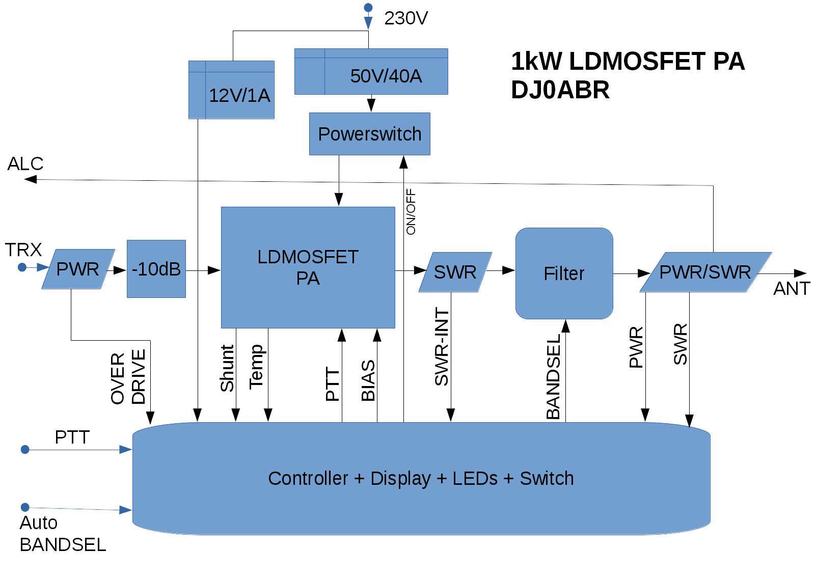
Here is the overview of the complete unit:
Protective devices:
- Input power monitoring. Turns off the PA and warns if the input is overdriven.
- Monitoring if the correct low pass filter is activated.
- Measurement of the antenna SWR
- Current consumption
- Voltage from power supply
- heat sink temperature
as soon as a dangerous situation occurs the 50V power supply is switched off. The 12V power supply remains in operation to maintain the monitoring functions.
LEDs:
- ON
- TX
- 160m
- 80m
- 60+40m
- 30+20m
- 17+15m
- 12+10m
- temperature error
- too high antenna SWR
- overcurrent
- overvoltage
- filter SWR too high
Switch:
- on/off
- Standby
- Error reset
- Band selection (Auto, or one of the bands, 7-position rotary switch)
Power supply:
Power supply 12V/1A for the control unit and the relays. Power supply 50V/40A for the power amplifier. Power supply with input for emergency shutdown Cooling:
The first tests have shown that air cooling is sufficient for SSB. Longer continuous wave operation (e.g. 10m FM) is not possible with it. Also, all loud fans should be banned from the shack.
Therefore:
Watercooling: In the copper plate, where the LDMOSFET is soldered, channels are milled on the backside and afterwards closed with a lid. Beginning and end of the channels get a hose connection.
Whether the power supplies can be integrated into the water cooling must first be investigated,


